


 The Government Circuit: Driving Resiliency and Economic Security on Both Sides of the Atlantic
 American Made Advocacy: Taking the Fight to Capitol Hill
 Defense Speak Interpreted: SWaPing Nanosatellites for Defense Systems
Pioneer Circuits’ Solutions Used in NASA's PUFFER Collapsible Bot
February 5, 2018 | Pioneer CircuitsEstimated reading time: 2 minutes
The PUFFER (Pop-Up Flat Folding Explorer Robot) collapsible micro-rover is a part of NASA’s “Game Changing Development Program.” It is a compact rover that will ride on board with future space vehicles to land on space bodies such as planets and asteroids for photographs and microanalysis.
Figure 1: The original PUFFER prototype before working with Pioneer Circuits for the new hinge technology.
The PUFFER micro-rover utilizes a new, patented hinge technology containing a high-temperature woven fabric that is compatible with PWB rigid-flex manufacturing. JPL utilized Pioneer Circuits’ concurrent engineering services to help with the new developments that were a key enabler for the PUFFER project.
The Challenge
The PUFFER’s concept addresses the challenge of developing robotic mobility in space exploration. The PUFFER challenge was to design a micro-rover capable of surviving the harsh environments of deep space while also being able to collapse and fold into more compact forms that will fit into small areas for detailed photographs and surface analysis.
The original PUFFER prototypes were having issues with passing their cycle and drop test operations. Design challenges included the mechanical design of the rigid-flex PCB joints to be able to work on a repeatedly folding robot structure, and for the PCB’s copper traces to last the lifetime of the rover. The original materials used for the joints were not compatible with current PCB manufacturing processes, and the PUFFER was only able to withstand 1,000 test cycles—a very conservative number for a Mars application.
Through concurrent engineering, Pioneer Circuits found the material and developed a high-temperature woven fabric hinge technology that is compatible with PCB rigid-flex manufacturing. The rigid-flex circuit technology is integrated into a highly reliable, composite structure that is the first origami micro-rover configuration ever developed.
Figure 2: A close-up of Pioneer Circuits and JPL’S hinge technology with woven fabric.
To make the technology possible, Pioneer Circuits developed new bonding and process capabilities that are compatible with this unique challenge. Integration of the high-temperature woven material as a layer in the PCB stack-up allowed the mechanical and electrical functions to overcome limitations of typical polyimide builds. Using the material as a hinge would makes the PUFFER more reliable and able to repeatedly collapse without damaging the copper traces. The new PUFFER design was capable of withstanding drop-testing that simulated the harsh space body environments, and was is able withstand over 5,000 cycle tests—500% more than the original designs.
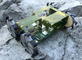
Figure 3: The final full and collapsed version of the PUFFER microrover.
Impact
Pioneer Circuits’ work with JPL on the development of the PUFFER has resulted in technology that is now being patented. The PUFFER micro-rover will now be able to ride on board with future space missions for thorough surface analysis. The collapsing capability allows the PUFFER’s microcamera to focus for microanalysis. This “Game Changing” development will give NASA and JPL a less-expensive opportunity to explore the surfaces of space that were never before reached.
Share on:


Suggested Items
Insulectro’s 'Storekeepers' Extend Their Welcome to Technology Village at IPC APEX EXPO
04/03/2024 | InsulectroInsulectro, the largest distributor of materials for use in the manufacture of PCBs and printed electronics, welcomes attendees to its TECHNOLOGY VILLAGE during this year’s IPC APEX EXPO at the Anaheim Convention Center, April 9-11, 2024.
ENNOVI Introduces a New Flexible Circuit Production Process for Low Voltage Connectivity in EV Battery Cell Contacting Systems
04/03/2024 | PRNewswireENNOVI, a mobility electrification solutions partner, introduces a more advanced and sustainable way of producing flexible circuits for low voltage signals in electric vehicle (EV) battery cell contacting systems.
Heavy Copper PCBs: Bridging the Gap Between Design and Fabrication, Part 1
04/01/2024 | Yash Sutariya, Saturn Electronics ServicesThey call me Sparky. This is due to my talent for getting shocked by a variety of voltages and because I cannot seem to keep my hands out of power control cabinets. While I do not have the time to throw the knife switch to the off position, that doesn’t stop me from sticking screwdrivers into the fuse boxes. In all honesty, I’m lucky to be alive. Fortunately, I also have a talent for building high-voltage heavy copper circuit boards. Since this is where I spend most of my time, I can guide you through some potential design for manufacturability (DFM) hazards you may encounter with heavy copper design.
Trouble in Your Tank: Supporting IC Substrates and Advanced Packaging, Part 5
03/19/2024 | Michael Carano -- Column: Trouble in Your TankDirect metallization systems based on conductive graphite or carbon dispersion are quickly gaining acceptance worldwide. Indeed, the environmental and productivity gains one can achieve with these processes are outstanding. In today’s highly competitive and litigious environment, direct metallization reduces costs associated with compliance, waste treatment, and legal issues related to chemical exposure. What makes these processes leaders in the direct metallization space?
AT&S Shines with Purest Copper on World Recycling Day
03/18/2024 | AT&SThe Styrian microelectronics specialist AT&S is taking World Recycling Day as an opportunity to review the progress that has been made in recent months at its sites around the world in terms of the efficient use of resources: