


 The Government Circuit: Driving Resiliency and Economic Security on Both Sides of the Atlantic
 American Made Advocacy: Taking the Fight to Capitol Hill
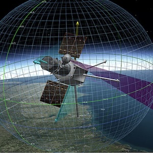
 Defense Speak Interpreted: SWaPing Nanosatellites for Defense Systems
2D Crystals Conforming to 3D Curves Create Strain for Engineering Quantum Devices
June 4, 2019 | ORNLEstimated reading time: 5 minutes
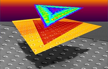
A team led by scientists at the Department of Energy’s Oak Ridge National Laboratory explored how atomically thin two-dimensional (2D) crystals can grow over 3D objects and how the curvature of those objects can stretch and strain the crystals. The findings, publishedin Science Advances, point to a strategy for engineering strain directly during the growth of atomically thin crystals to fabricate single photon emitters for quantum information processing.
Image Caption: Strain-tolerant, triangular, monolayer crystals of WS2 were grown on SiO2 substrates patterned with donut-shaped pillars, as shown in scanning electron microscope (bottom) and atomic force microscope (middle) image elements. The curvature of the pillars induced strain in the overlying crystals that locally altered their optoelectronic properties, as shown in bright regions of photoluminescence (top). Credit: Christopher Rouleau/Oak Ridge National Laboratory, U.S. Dept. of Energy
The team first explored growth of the flat crystals on substrates patterned with sharp steps and trenches. Surprisingly, the crystals conformally grew up and down these flat obstacles without changing their properties or growth rates. However, curvy surfaces required the crystals to stretch as they grew to maintain their crystal structure. This growth of 2D crystals into the third dimension presented a fascinating opportunity.
“You can engineer how much strain you impart to a crystal by designing objects for them to grow over,” said Kai Xiao, who with ORNL colleagues David Geohegan and postdoctoral researcher Kai Wang (now at Intel) conceived the study. “Strain is one way to make ‘hot spots’ for single photon emitters.”
Conformal growth of perfect 2D crystals over 3D objects has the promise to localize strain to create high-fidelity arrays of single photon emitters. Stretching or compressing the crystal lattice changes the material’s band gap, the energy gap between the valence and conduction bands of electrons, which largely determines a material’s optoelectronic properties. Using strain engineering, researchers can funnel charge carriers to recombine precisely where desired in the crystal instead of at random defect locations. By tailoring curved objects to localize strain in the crystal, and then measuring resulting shifts in optical properties, the experimentalists compelled co-authors at Rice University—theorists Henry Yu, Nitant Gupta and Boris Yakobson—to simulate and map how curvature induces strain during crystal growth.
At ORNL, Wang and Xiao designed experiments with Bernadeta Srijanto to explore the growth of 2D crystals over lithographically patterned arrays of nanoscale shapes. Srijanto first used photolithography masks to protect certain areas of a silicon oxide surface during exposure to light, and then etched away the exposed surfaces to leave vertically standingshapes, including donuts, cones and steps. Wang and another postdoctoral researcher, Xufan Li (now at Honda Research Institute), then inserted the substrates into a furnace where vaporized tungsten oxide and sulfur reacted to deposit tungsten disulfide on the substrates as monolayer crystals. The crystals grew as an orderly lattice of atoms in perfect triangular tiles that grew larger with time by adding row after row of atoms to their outer edges. While the 2D crystals seemed to effortlessly fold like paper over tall steps and sharp trenches, growth over curved objects forced the crystals to stretch to maintain their triangular shape.
The scientists found that “donuts” 40 nanometers high were great candidates for single photon emitters because the crystals could reliably tolerate the strain they induced, and the maximum strain was precisely in the “hole” of the donut, as measured by shifts in the photoluminescence and Raman scattering. In the future, arrays of donuts or other structures could be patterned anywhere that quantum emitters are desired before the crystals are grown.
Wang and ORNL co-author Alex Puretzky used photoluminescence mapping to reveal where the crystals nucleated and how fast each edge of the triangular crystal progressed as it grew over the donuts. After careful analysis of the images, they were surprised to discover that although the crystals maintained their perfect shapes, the edges of crystals that had been strained by donuts grew faster.
To explain this acceleration, Puretzky developed a crystal growth model, and colleague Mina Yoon conducted first-principles calculations. Their work showed that strain is more likely to induce defects on the growing edge of a crystal. These defects can multiply the number of nucleation sites that seed crystal growth along an edge, allowing it to grow faster than before.
The reason crystals can grow easily up and down deep trenches, but become strained by shallow donuts, has to do with conformity and curvature. Imagine wrapping presents. Boxes are easy to wrap because the paper can fold to conform to the shape. But an irregularly shaped object with curves, such as an unboxed mug, is impossible to wrap conformally (to avoid tearing the paper, you would have to be able to stretch it like plastic wrap.)
The 2D crystals also stretch to conform to the substrate’s curves. Eventually, however, the strain becomes too great and the crystals split to release the strain, atomic force microscopy and other techniques revealed. After the crystal cracks, growth of the still-strained material proceeds in different directions for each new arm. At Nanjing University of Aeronautics and Astronautics, Zhili Hu performed phase-field simulations of crystal branching. Xiang Gao of ORNL and Mengkun Tian (formerly of the University of Tennessee) analyzed the atomic structure of the crystals by scanning transmission electron microscopy.
“The results present exciting opportunities to take two-dimensional materials and vertically integrate them into the third dimension for next-generation electronics,” said Xiao.
Next the researchers will explore whether strain can enhance the performance of tailored materials. “We’re exploring how the strain of the crystal can make it easier to induce a phase change so the crystal can take on entirely new properties,” Xiao said. “At the Center for Nanophase Materials Sciences, we’re developing tools that will allow us to probe these structures and their quantum information aspects.”
Share on:


Suggested Items
Groundbreaking Ceremony Marks the Beginning of a New Era for Newccess Industrial; The Construction of the MINGXIN Building
04/12/2024 | Newccess IndustrialOn a clear and sunny day in March, the groundbreaking ceremony for the MINGXIN Building took place in Shenzhen, China. This moment marked the official commencement of construction for a project that will reshape the semiconductor materials industry.
The Need for a Holistic Global Sustainability Standard
04/10/2024 | Michael Ford, Aegis SoftwareNo one can deny that the resources of our fragile planet are finite. The environment seems like a third party, subject to constant degradation. We’re acutely aware of the effects of pollution on our climate, and despite our “throw-away” culture, recycling and recovery of materials has remained relatively expensive, even as we use more energy just to survive.
iNEMI Publishes Four Roadmap Topics
04/04/2024 | iNEMIThe International Electronics Manufacturing Initiative (iNEMI) announces the availability of the first roadmap topics in the new iNEMI Roadmap format. Printed circuit boards, sustainable electronics, smart manufacturing, and mmWave materials and test are now available online.
Insulectro’s 'Storekeepers' Extend Their Welcome to Technology Village at IPC APEX EXPO
04/03/2024 | InsulectroInsulectro, the largest distributor of materials for use in the manufacture of PCBs and printed electronics, welcomes attendees to its TECHNOLOGY VILLAGE during this year’s IPC APEX EXPO at the Anaheim Convention Center, April 9-11, 2024.
Checking In With ICAPE Group
04/03/2024 | Nolan Johnson, I-Connect007ICAPE Group’s field application engineer Erik Pederson drills down on sustainability, supply chain resiliency, and what value engineering really looks like in this exclusive interview. Founded in 1999, European-based ICAPE Group provides 21 million printed circuit boards and over six million technical parts to manufacturers every month. With 30 PCB manufacturing partners globally and 50 partners providing a wide array of technical parts, ICAPE Group has operations in China, Taiwan, Thailand, South Korea, Vietnam, South Africa, Europe, Mexico, and the United States. The company also focuses on the value proposition for its customers.