


 The Government Circuit: Driving Resiliency and Economic Security on Both Sides of the Atlantic
 American Made Advocacy: Taking the Fight to Capitol Hill
 Defense Speak Interpreted: SWaPing Nanosatellites for Defense Systems
Ayar Labs Adds $25 Million in Expansion of Its $130 Million Series C
May 25, 2023 | Business WireEstimated reading time: 2 minutes
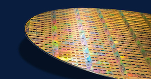
Ayar Labs, a leader in silicon photonics for chip-to-chip connectivity, announced it has raised an additional $25 million in Series C1 funding, bringing its total Series C raise to $155 million. The oversubscribed up round was led by new investor Capital TEN. VentureTech Alliance also entered the Series C expansion that included participation by previous investors Boardman Bay Capital Management, IAG Capital Partners, NVIDIA, and Tyche Partners. Existing strategic and financial investors include Applied Ventures, GlobalFoundries, Hewlett Packard Pathfinder, Intel Capital and Lockheed Martin Ventures.
“We believe that future computing solutions will include large-scale use of silicon photonics for data communications, and have been following Ayar Labs for some time now,” said Pin-Nan Tseng, General Partner at Capital TEN. “Given our deep expertise in the semiconductor industry and the Taiwan semiconductor ecosystem, we believe Ayar Labs has the technology solution, people, capital, and broad support to lead in the transition from copper to optical interconnects for scale-out computing and memory applications.”
Ayar Labs’ patented optical I/O approach uses industry-standard, cost-effective silicon processing techniques to replace traditional electrical I/O with fast, high-density, low power optical I/O chiplets and multi-wavelength light sources. Moving data between chips using light instead of electricity breaks the performance, power, and distance limitations of copper interconnect, critical for latency-sensitive applications such as high performance computing, AI and machine learning. Optical I/O will also impact other areas that require rapid transfer of data, such as cloud and data center, telecommunications, and aerospace and defense.
“We’re extremely pleased with the ongoing interest and financing we’ve received from leaders in the semiconductor industry,” said Charles Wuischpard, CEO of Ayar Labs. “This C1 adds sophisticated investor partners that will allow us to accelerate our strategic roadmap, and is further validation of our technology and plan to bring silicon photonics-based interconnect solutions to market at scale.”
Ayar Labs will use the funds to accelerate the implementation and commercialization of its optical I/O solutions to address the power consumption, latency, reach and system bandwidth bottlenecks that threaten future advances in generative AI, while also expanding the company's product offerings and development efforts.
NVIDIA, which participated in Ayar Labs’ earlier Series C raise in April 2022, increased its investment in the company.
“NVIDIA is reimagining the data center with integrated hardware, software and networking for accelerated computing,” said Craig Thompson, Vice President of Business Development, Networking Business Unit at NVIDIA. “Generative AI models with trillions of parameters are accelerating demand for this platform, which is why we are increasing our investment in Ayar Labs.”
Recently named one of America’s Best Startup Employers by Forbes, the funds will also help the company increase hiring plans by up to 50 percent this year. Ayar Labs has received a number of other accolades in recent months. The company was recognized as an honoree in Fast Company’s most recent “Next Big Things in Tech” awards. In addition, Mark Wade, Ayar Labs’ Co-Founder, CTO and Senior Vice President of Engineering, was recently appointed to Global Semiconductor Alliance’s CTO Council. Wade was also recently named to Electro Optics’ inaugural “The Photonics 100 2023” list.
Share on:


Suggested Items
Insulectro’s 'Storekeepers' Extend Their Welcome to Technology Village at IPC APEX EXPO
04/03/2024 | InsulectroInsulectro, the largest distributor of materials for use in the manufacture of PCBs and printed electronics, welcomes attendees to its TECHNOLOGY VILLAGE during this year’s IPC APEX EXPO at the Anaheim Convention Center, April 9-11, 2024.
ENNOVI Introduces a New Flexible Circuit Production Process for Low Voltage Connectivity in EV Battery Cell Contacting Systems
04/03/2024 | PRNewswireENNOVI, a mobility electrification solutions partner, introduces a more advanced and sustainable way of producing flexible circuits for low voltage signals in electric vehicle (EV) battery cell contacting systems.
Heavy Copper PCBs: Bridging the Gap Between Design and Fabrication, Part 1
04/01/2024 | Yash Sutariya, Saturn Electronics ServicesThey call me Sparky. This is due to my talent for getting shocked by a variety of voltages and because I cannot seem to keep my hands out of power control cabinets. While I do not have the time to throw the knife switch to the off position, that doesn’t stop me from sticking screwdrivers into the fuse boxes. In all honesty, I’m lucky to be alive. Fortunately, I also have a talent for building high-voltage heavy copper circuit boards. Since this is where I spend most of my time, I can guide you through some potential design for manufacturability (DFM) hazards you may encounter with heavy copper design.
Trouble in Your Tank: Supporting IC Substrates and Advanced Packaging, Part 5
03/19/2024 | Michael Carano -- Column: Trouble in Your TankDirect metallization systems based on conductive graphite or carbon dispersion are quickly gaining acceptance worldwide. Indeed, the environmental and productivity gains one can achieve with these processes are outstanding. In today’s highly competitive and litigious environment, direct metallization reduces costs associated with compliance, waste treatment, and legal issues related to chemical exposure. What makes these processes leaders in the direct metallization space?
AT&S Shines with Purest Copper on World Recycling Day
03/18/2024 | AT&SThe Styrian microelectronics specialist AT&S is taking World Recycling Day as an opportunity to review the progress that has been made in recent months at its sites around the world in terms of the efficient use of resources: