


 The Government Circuit: Driving Resiliency and Economic Security on Both Sides of the Atlantic
 American Made Advocacy: Taking the Fight to Capitol Hill
 Defense Speak Interpreted: SWaPing Nanosatellites for Defense Systems
Intel Joins DARPA’s Space-BACN to Accelerate Inter-Satellite Communications
October 12, 2022 | IntelEstimated reading time: 3 minutes

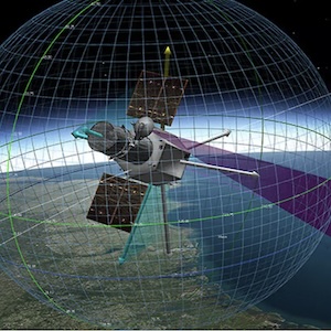
The U.S. Defense Advanced Research Projects Agency (DARPA) has selected Intel for Phase 1 of the Space-Based Adaptive Communications Node (Space-BACN) program, which aims to create a low-cost, reconfigurable optical communications terminal that will translate information between diverse satellite constellations. A Space-BACN satellite terminal will enable communications between satellite constellations, enabling data to be sent anywhere around the planet at the speed of light.
“Intel’s vision is to create world-changing technology that improves the life of every person on the planet. This program helps us to deliver on that vision by enabling global connectivity from space to anywhere across the planet – enabling broadband services and the IoT where not just every person but everything is connected,” says Sergey Shumarayev, Intel senior principal engineer and principal investigator in the Programmable Solutions CTO Group
DARPA is planning for a future where tens of thousands of satellites from multiple private sector organizations deliver broadband services from low earth orbit (LEO). The goal of Space-BACN is to create an “internet” of satellites, enabling seamless communication between military/government and commercial/civil satellite constellations.
The program will facilitate collaboration among partners to ensure that the terminal being designed is reconfigurable to provide interoperability among the participating constellation providers.
There are three technical areas in the program.
DARPA selected Intel for Technical Area 2 (TA2) along with II-VI Aerospace and Defense and Arizona State University to design a reconfigurable optical modem that will support both current and new communication standards and protocols to enable interoperability among satellite constellations.
Technical Area 1 (TA1) focuses on the development of an optical aperture or “head,” which is responsible for pointing acquisition and tracking, as well as the optical transmit and receive functions. DARPA has selected the following organizations for this technical area: CACI Inc., MBRYONICS and Mynaric.
TA1 will interface to TA2 using single-mode optical fiber.
In Technical Area 3 (TA3), DARPA selected constellation providers – Space Exploration Technologies (SpaceX), Telesat, SpaceLink, Viasat and Kuiper Government Solutions (KGS) LLC (an Amazon subsidiary) – to identify critical command and control elements required to support cross-constellation optical intersatellite link communications and develop the schema necessary to interface between Space-BACN and commercial partner constellations.
Intel is developing its optical modem solution by bringing together experts from its field programmable gate array (FPGA) product group, packaging technologists from its Assembly Test Technology Development (ATTD) division and researchers from Intel Labs.
Based on its leading-edge low-power Intel® Agilex™ FPGA, Intel will also design three new chiplets that will be integrated using Intel’s embedded multi-die interconnect bridge (EMIB) and advanced interface bus (AIB) packaging technologies into a single multi-chip package (MCP) that includes:
- A DSP/FEC chiplet on Intel 3, the most advanced digital node, that enables low-power, high-speed digital signal processing.
- A data converter/TIA/driver chiplet on Intel 16, which provides the best-in-class FinFET RF signal processing for integration of high-speed data converters, TIAs and drivers.
- A PIC chiplet based on Tower Semiconductor photonic technologies that offers low-loss waveguides and options, such as V-groove, enabling automated high-volume fiber coupling integration and assembly.
Intel has commenced Phase 1 of the program where it will design each of the above chiplets and work with the other performers to fully define the interfaces between the system components in each of the other technical areas. Phase 1 will last 14 months and conclude with a preliminary design review.
At the completion of Phase 1, selected performers in the first two technical areas will participate in an 18-month Phase 2 to develop engineering design units of the optical terminal components, while performers in the third technical area will continue to evolve the schema to function in more challenging and dynamic scenarios.
Share on:


Suggested Items
Cicor Records Solid Growth in Q1
04/16/2024 | CicorThe Cicor Group continued to grow in the first three months of the year. Quarterly sales increased by 11.8% to CHF 107.3 million compared to the first quarter of the previous year (Q1/2023: CHF 96.0 million).
TT Electronics Awarded Contract with Kongsberg Defence and Aerospace
04/11/2024 | TT ElectronicsTT Electronics, a leading provider of global manufacturing solutions and engineered technologies, announced today that its Fairford UK business has been awarded a new contract with long-standing customer Kongsberg Defence and Aerospace (Kongsberg) for the production of complex cable harness solutions.
Cicor Successfully Completes Acquisition of TT Electronics IoT Solutions Ltd.
04/03/2024 | CicorThe Cicor Group has successfully completed the acquisition of TT Electronics IoT Solutions Ltd. with three production sites in the UK and China.
Absolute EMS Successfully Recertifies ISO 9001:2015 and AS9100 Standards
03/26/2024 | Absolute EMS, Inc.Absolute EMS, Inc., an award-winning EMS provider of turnkey contract manufacturing services, is proud to announce the successful recertification of its ISO 9001:2015 and AS9100 Rev D SAE International Aerospace Standards.
Arlon EMC Receives IPC-4101 QPL Recertification
03/20/2024 | Arlon Electronic MaterialsArlon Electronic Materials has successfully completed an intensive two-day recertification audit by IPC Validation Services that examined Arlon’s manufacturing processes and testing procedures to assure that they are in conformance to the requirements of IPC-4101E-WAM1, the Specification for Base Materials for Rigid and Multilayer Printed Boards.