


 The Government Circuit: Driving Resiliency and Economic Security on Both Sides of the Atlantic
 American Made Advocacy: Taking the Fight to Capitol Hill
 Defense Speak Interpreted: SWaPing Nanosatellites for Defense Systems
DARPA Making Progress on Miniaturized Atomic Clocks for Future PNT Applications
August 22, 2019 | DARPAEstimated reading time: 5 minutes
Many of today’s communications, navigation, financial transaction, distributed cloud, and defense applications rely on the precision timing of atomic clocks—or clocks that track time based on the oscillation of atoms with the highest degrees of accuracy. Harnessing the power of atoms for precise timing requires a host of sophisticated and bulky technologies that are costly to develop and consume large amounts of energy. New applications and technologies like 5G networks and GPS alternatives will require precise timekeeping on portable platforms, driving a demand for miniaturized atomic clocks with a high degree of performance.
Over the past few decades, DARPA has invested heavily in the advancement and miniaturization of atomic clock technology, generating chip-scale atomic clocks (CSACs) that are now commercially available and offer unprecedented timing stability for their size, weight, and power (SWaP). However, the performance of these first-generation CSACs are fundamentally limited due to the physics associated with their designs. Calibration requirements and frequency drift can generate timing errors, making it difficult to achieve the highest degrees of accuracy and reliability in a portable package. DARPA’s Atomic Clock with Enhanced Stability (ACES) program is exploring the development of next-generation, battery-powered CSACs with 1000x improvement in key performance parameters over existing options.
“Shrinking atomic clocks from large cesium beam tubes to chip-scale devices without eroding performance requires a rethinking of a number of critical components, including vacuum pumps and optical isolators as well as new approaches to component integration,” said Dr. John Burke, the program manager leading ACES in DARPA’s Microsystems Technology Office (MTO). “The target metrics we outlined for the ACES program are lofty, but as we enter the third phase of the program, researchers are already demonstrating engineering successes including reduced SWaP, lab-proven atomic clock technologies, as well as early prototypes of future clock architectures.”
Through the exploration of alternative physics architectures and novel component technologies, three sets of researchers have demonstrated early progress towards creating CSACs with 1000x improvement in temperature control, aging, and retrace.
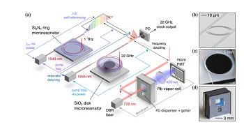
A paper recently published in Optica highlights recent progress made by a team of researchers from the National Institute of Standards and Technology (NIST), with support from researchers at the California Institute of Technology, Stanford University, and Charles Stark Draper Laboratories. The team has demonstrated an experimental optical atomic clock that is comprised of only three small chips and supporting electronics and optics. Unlike standard atom clocks that operate at microwave frequencies and track the vibrations of cesium atoms, optical atomic clocks run at higher frequencies, offering greater precision because they divide time into smaller units. The NIST team’s clock uses a laser to track the oscillations of rubidium atoms confined in a vapor cell—or tiny glass container—that is 3 millimeters across sitting on top of a silicon chip. Within the clock’s chip-based “heart,” two frequency combs act like gears to convert the rubidium atoms’ high-frequency optical “ticks” to the lower microwave frequency, which is used by most PNT applications to track time. In addition to providing a higher-degree of accuracy (roughly 50 times better than the current cesium-based CSACs), the experimental clock uses very little power—just 275 milliwatts.
In addition to successfully demonstrating a chip-scale optical clock, the NIST team was able to microfabricate all of the key components, much in the same way that computer chips are fabricated. This enables further integration of the electronics and optics while creating a potential path towards mass production and commercialization.
Figure 1: Schematic of the microfabricated photonic optical atomic clock developed by NIST, California Institute of Technology, Stanford University, and Charles Stark Draper Laboratories. Source: NIST
A second team of researchers from Honeywell, working in partnership with University of California, Santa Barbara, is developing precision atomic sensors to support the development of a miniature atomic clock.
Page 1 of 2
Share on:


Suggested Items
Terran Orbital’s GEOStare SV2 Captures 3 Years of Success in High-Resolution Imaging
05/17/2024 | BUSINESS WIRETerran Orbital Corporation, a global leader in satellite-based solutions primarily serving the aerospace and defense industries, celebrates the 3rd anniversary of its successful GEOStare SV2 mission. Launched on May 15, 2021, from NASA’s Kennedy Space Center in Florida, GEOStare SV2 has surpassed expectations, delivering exceptional results for commercial satellite imagery.
Indium Experts to Present on High-Temperature, Lead-Free Solder Paste and High Reliability Liquid Metal Alloys Poster at ECTC
05/16/2024 | Indium CorporationIndium Corporation Research Associate Kyle Aserian will deliver a presentation at the 74th Electronic Components and Technology Conference (ECTC) on May 31, in Denver, Colorado.
Siemens, Foxconn Team Up to Optimize Forward-thinking Manufacturing
05/16/2024 | FoxconnSiemens AG, a leading technology company, and Hon Hai Technology Group (Foxconn), the world’s largest electronics manufacturer, have signed a memorandum of understanding (MoU) to drive digital transformation and sustainability in smart manufacturing platforms.
TactoTek Licenses IMSE Technology to Polestar for Sustainable Electronics Design Innovation
05/15/2024 | TactoTekPolestar, the Swedish electric performance car brand, and Finnish smart surface pioneer TactoTek, have entered a collaboration to explore integration of Injection Molded Structural Electronics (IMSE) technology into Polestar’s vehicle programs.
SiPearl: Partnership with Samsung Electronics for built-in HBM in Rhea
05/14/2024 | BUSINESS WIRESiPearl, the company building the high-performance low-power European microprocessor for HPC and AI inference, has signed a partnership with Samsung Electronics Co. Ltd., a world leader in advanced memory technology, to equip its Rhea series with Samsung’s advanced memory solution ideal for HPC and AI applications.