


 The Government Circuit: Driving Resiliency and Economic Security on Both Sides of the Atlantic
 American Made Advocacy: Taking the Fight to Capitol Hill
 Defense Speak Interpreted: SWaPing Nanosatellites for Defense Systems
DARPA Making Progress on Miniaturized Atomic Clocks for Future PNT Applications
August 22, 2019 | DARPAEstimated reading time: 5 minutes
Many of today’s communications, navigation, financial transaction, distributed cloud, and defense applications rely on the precision timing of atomic clocks—or clocks that track time based on the oscillation of atoms with the highest degrees of accuracy. Harnessing the power of atoms for precise timing requires a host of sophisticated and bulky technologies that are costly to develop and consume large amounts of energy. New applications and technologies like 5G networks and GPS alternatives will require precise timekeeping on portable platforms, driving a demand for miniaturized atomic clocks with a high degree of performance.
Over the past few decades, DARPA has invested heavily in the advancement and miniaturization of atomic clock technology, generating chip-scale atomic clocks (CSACs) that are now commercially available and offer unprecedented timing stability for their size, weight, and power (SWaP). However, the performance of these first-generation CSACs are fundamentally limited due to the physics associated with their designs. Calibration requirements and frequency drift can generate timing errors, making it difficult to achieve the highest degrees of accuracy and reliability in a portable package. DARPA’s Atomic Clock with Enhanced Stability (ACES) program is exploring the development of next-generation, battery-powered CSACs with 1000x improvement in key performance parameters over existing options.
“Shrinking atomic clocks from large cesium beam tubes to chip-scale devices without eroding performance requires a rethinking of a number of critical components, including vacuum pumps and optical isolators as well as new approaches to component integration,” said Dr. John Burke, the program manager leading ACES in DARPA’s Microsystems Technology Office (MTO). “The target metrics we outlined for the ACES program are lofty, but as we enter the third phase of the program, researchers are already demonstrating engineering successes including reduced SWaP, lab-proven atomic clock technologies, as well as early prototypes of future clock architectures.”
Through the exploration of alternative physics architectures and novel component technologies, three sets of researchers have demonstrated early progress towards creating CSACs with 1000x improvement in temperature control, aging, and retrace.
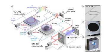
A paper recently published in Optica highlights recent progress made by a team of researchers from the National Institute of Standards and Technology (NIST), with support from researchers at the California Institute of Technology, Stanford University, and Charles Stark Draper Laboratories. The team has demonstrated an experimental optical atomic clock that is comprised of only three small chips and supporting electronics and optics. Unlike standard atom clocks that operate at microwave frequencies and track the vibrations of cesium atoms, optical atomic clocks run at higher frequencies, offering greater precision because they divide time into smaller units. The NIST team’s clock uses a laser to track the oscillations of rubidium atoms confined in a vapor cell—or tiny glass container—that is 3 millimeters across sitting on top of a silicon chip. Within the clock’s chip-based “heart,” two frequency combs act like gears to convert the rubidium atoms’ high-frequency optical “ticks” to the lower microwave frequency, which is used by most PNT applications to track time. In addition to providing a higher-degree of accuracy (roughly 50 times better than the current cesium-based CSACs), the experimental clock uses very little power—just 275 milliwatts.
In addition to successfully demonstrating a chip-scale optical clock, the NIST team was able to microfabricate all of the key components, much in the same way that computer chips are fabricated. This enables further integration of the electronics and optics while creating a potential path towards mass production and commercialization.
Figure 1: Schematic of the microfabricated photonic optical atomic clock developed by NIST, California Institute of Technology, Stanford University, and Charles Stark Draper Laboratories. Source: NIST
A second team of researchers from Honeywell, working in partnership with University of California, Santa Barbara, is developing precision atomic sensors to support the development of a miniature atomic clock.
Page 1 of 2
Share on:


Suggested Items
Warm Windows and Streamlined Skin Patches – IDTechEx Explores Flexible and Printed Electronics
04/26/2024 | IDTechExFlexible and printed electronics can be integrated into cars and homes to create modern aesthetics that are beneficial and easy to use. From luminous car controls to food labels that communicate the quality of food, the uses of this technology are endless and can upgrade many areas of everyday life.
iNEMI Packaging Tech Topic Series: Role of EDA in Advanced Semiconductor Packaging
04/26/2024 | iNEMIAdvanced semiconductor packaging with heterogenous integration has made on-package integration of multiple chips a crucial part of finding alternatives to transistor scaling. Historically, EDA tools for front-end and back-end design have evolved separately; however, design complexity and the increased number of die-to-die or die-to-substrate interconnections has led to the need for EDA tools that can support integration of overall design planning, implementation, and system analysis in a single cockpit.
Koh Young Showcases Award-winning Inspection Solutions at SMTconnect with SmartRep in Hall 4A.225
04/25/2024 | Koh Young TechnologyKoh Young Technology, the industry leader in True 3D measurement-based inspection solutions, will showcase an array of award-winning inspection and measurement solutions at SMTconnect alongside its sales partner, SmartRep, in booth 4A.225 at NürnbergMesse from June 11-13, 2023. The following offers a glimpse into what Koh Young will present at the tradeshow:
Real Time with… IPC APEX EXPO 2024: Plasmatreat: Innovative Surface Preparation Solutions
04/25/2024 | Real Time with...IPC APEX EXPOIn this interview, Editor Nolan Johnson speaks with Hardev Grewal, CEO and president of Plasmatreat, a developer of atmospheric plasma solutions. Plasmatreat uses clean compressed air and electricity to create plasma, offering environmentally friendly methods for surface preparation. Their technology measures plasma density for process optimization and can remove organic micro-contamination. Nolan and Hardev also discuss REDOX-Tool, a new technology for removing metal oxides.
Nanotechnology Market to Surpass $53.51 Billion by 2031
04/25/2024 | PRNewswireSkyQuest projects that the nanotechnology market will attain a value of USD 53.51 billion by 2031, with a CAGR of 36.4% over the forecast period (2024-2031).